We understood that Intel’s Meteor Lake would start an essential brand-new period with a style that stacks a couple of “chiplets” like pancakes into a single next-generation PC processor. And now we understand something else: Among those chiplets will house a very low-power CPU that can keep a laptop computer ticking without as much of a struck on its battery.
Intel divulged the brand-new style information at its Development conference Tuesday in addition to some information on Meteor Lake’s followers, Arrow Lake, Lunar Lake, and Panther Lake President Pat Gelsinger likewise provided a status report on his multiyear effort to recover Intel’s lost processor style and production management Meteor Lake, set to deliver on December 14 and for this year’s last crop of laptop computers, is a focal point of one stage of that effort.
Apple’s M series of processors, powering MacBook laptop computers with long battery life and no loud cooling fans, have actually shown the benefits of processor performance. Meteor Lake will resist in 2 essential methods, and if Intel provides as assured, that need to indicate much better laptop computers for countless us who utilize Windows laptop computers.
See likewise: Inside Intel’s Chip Factory, I Saw the Future. It appears Old Glass
First is an upgrade to the primary brain inside Meteor Lake’s style, a chiplet called the “calculate tile” that consists of a collection of CPU (main processing system) cores. Just like Intel’s existing Alder Lake processors, officially called 13th-generation Core, the processor will consist of both huge high-performance CPU cores for the most requiring jobs and smaller sized performance cores for lower-priority work and much better battery life. Meteor Lake’s CPU cores have actually upgraded styles that are more effective which are developed utilizing the brand-new Intel 4 production procedure that likewise is more effective, Intel stated.
However tucked into another tile, the system-on-a-chip (SOC) chiplet, there are much more effective CPU cores on a “low power island.” The processor mixes software application jobs amongst the efficiency and performance cores lot of times each 2nd to get the very best outcomes, and unused cores can be idled to conserve battery power.
” For finest performance, you’ll see work bounced around the cores a lot,” stated Tim Wilson, the engineering group vice president who led the SOC style. “For a great deal of individuals, battery life today is as essential as efficiency in their PC. Meteor Lake will shine on both.”
The chip likewise will bring brand-new capabilities to speed up graphics on its graphics processing system and expert system jobs on its neural processing system Both of those are crucial measurements of efficiency in contemporary makers, especially higher-end computer systems utilized for jobs like video gaming or video and picture modifying.
PCs aren’t effective adequate to run the highest-end big language designs like ChatGPT, however AI innovation is utilized for jobs like choosing photo topics in Adobe Lightroom and eliminating backgrounds and audio sound in Microsoft Teams videoconferences.
Brand-new graphics brains for Meteor Lake
With the Meteor Lake processors, which the business will offer under the Core Ultra brand name, Intel debuts its next generation of integrated graphics, Xe LPG. LPG runs more effectively than the previous generation’s Xe LP, in theory reaching greater frequencies at lower voltages for much better battery life.
LPG likewise brings some essential abilities from the business’s Xe HPG discrete graphics to the GPU chiplet.
They consist of all the fundamentals for supporting DirectX 12 Ultimate: devoted raytracing accelerators (one per graphics core, with approximately 8 cores per GPU) and assistance for mesh shaders, variable rate shading and sampler feedback.
The architecture likewise includes assistance for Intel’s upscaling innovation, XeSS ( Xe Super Testing), which is partly depending on AI. XeSS makes it possible for Stamina Video gaming mode– an Intel-specific power-saving mode that integrates aggressive upscaling with CPU throttling for those times when you frantically require to make it to a checkpoint on battery.
With LPG, laptop computers utilizing Core Ultra chips get an increase to supporting a single 8K 60Hz with 10-bit HDR decoding and encoding or 4 4K 60Hz HDR, 1440p 360Hz or 1080p 360Hz displays, in addition to HDMI 2.1.
TSMC, Intel’s rival and partner
Intel is under intense competitive pressure. Throughout its years of stalled production development, Taiwan Semiconductor Production Co. (TSMC) and Samsung leapfrogged Intel’s when powerful innovation lead.
So did competitors that make chips. AMD made attacks into Intel’s market share, especially in the server market where information centers are loaded with countless high-end processors. Nvidia took advantage of explosive need for AI processors. And Apple disposed Intel processors, moving rather to its own M-series processors and providing engaging efficiency and lower power intake. TSMC develops the processors for all 3 of those significant Intel competitors.
I Got an Early Take a look at Intel’s Glass Product packaging Tech for Faster Chips.
However oddly, TSMC isn’t simply an Intel rival. It’s likewise a partner. It’s making the majority of the chiplets inside Meteor Lake.
TSMC is constructing Meteor Lake’s SOC tile– the chiplet that houses the low power island, AI accelerator, video decoder video and Wi-Fi system– on its N6 making procedure. That’s likewise utilized for the I/O tile, which manages input-output tasks like Thunderbolt and USB connections.
TSMC’s advanced N5 procedure is utilized to develop Meteor Lake’s Arc GPU system. It will provide two times the efficiency and two times the efficiency per watt as the 13th-gen Alder Lake processors, Intel stated.
Under Gelsinger, Intel is dealing with changing its own chipmaking company by ending up being a “foundry” like TSMC and Samsung that develops chips for other consumers. It’s drawn in a couple of customers, however business isn’t anticipated to get in earnest up until the Intel 18A making procedure gets here, arranged for 2024.
Chiplets ahoy
Meteor Lake’s “disaggregated” style, allowed by an Intel chiplet-stacking innovation called Foveros, signifies things to come for the processor market.
AMD is stacking quick memory caches into its high-end PC processors, and Apple’s M2 Ultra includes 2 M2 Max chips gotten in touch with a high-speed interaction bridge. However Intel is more aggressive with its chiplet method, in part due to the fact that of its requirement to attempt to reach rivals, Imaginative Techniques expert Ben Bajarin stated.
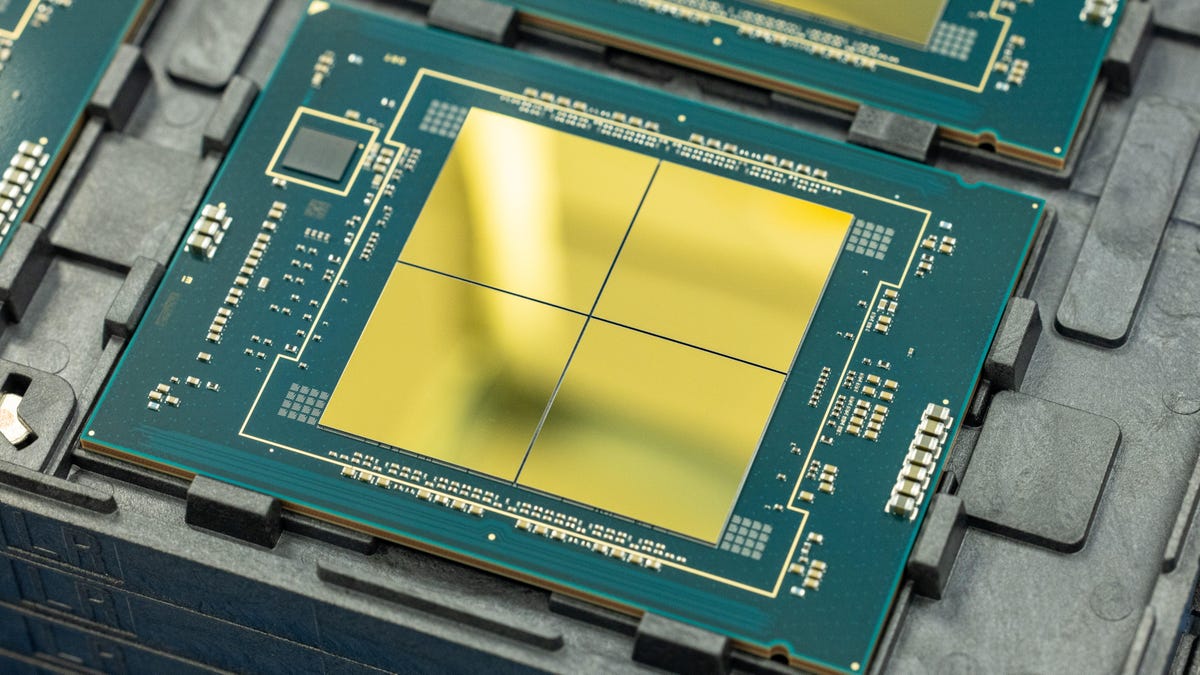
A real-world example of Intel’s product packaging innovation is Intel’s Sapphire Rapids, a big Xeon processor for information centers. Intel integrates 4 CPU tiles, each likewise called a die or chiplet, into one bigger processor. Intel’s EMIB (ingrained multidie adjoin bridge), a thin sliver of silicon below the edges where the tiles abut, provide information links throughout the processor so it acts like one bigger system.
With the Sapphire Rapids Xeon chip for information centers Intel started offering previously this year, then with Meteor Lake later on this year, the majority of the business’s 2 primary line of product will include processors made from numerous interlinked chiplets.
Product packaging various chiplets increases making expense and time, however it likewise uses a range of benefits. Various production procedures can be utilized for various chiplets to enhance qualities like expense, power intake and efficiency. And smaller sized chips are less vulnerable to making flaws.
And Intel’s glass substrate innovation, likewise detailed at the Development conference, leads the way for much more innovative chiplet techniques. That glass– a structure for the plan that houses a processor– uses much better speed, power and size benefits over today’s innovation.
Meteor Lake does not utilize glass substrates, which aren’t anticipated to get here up until later on this years, however it does show Intel’s product packaging ability. For instance, to combat the warping that indicates processors are a little bent like a potato chip, Intel utilizes variably sized solder balls to compensate and guarantee great electrical contacts.
Intel likewise can consume to 4 kinds of solder balls in its procedure, for instance sensibly utilizing more intricate copper core balls for power connections. The business displayed this “multiball” innovation in a trip of its advanced product packaging research study laboratories in Chandler, Arizona
” As we keep an eye out into the next 5 to ten years,” stated Tom Rucker, the vice president in charge of Intel’s assembly combination work, “that product packaging is going to end up being more vital.”